Les nouveaux usages d'aujourd'hui seront les business de demain.
Revue de presse sur les tendances et évolutions technologiques utiles.
http://theitwatcher.fr/.
SemiconductorsDesignNews The Rise of the Monolithic 3-D Chip
A lire sur: http://spectrum.ieee.org/semiconductors/design/the-rise-of-the-monolithic-3d-chip/
Researchers aim to ease miniaturization pressure with dense 3-D circuitry instead of stacked chips
By Rachel Courtland
Posted
Image: CEA-LetiTwo-story Circuit: Multistory circuits could let chipmakers increase the density of devices on a chip without having to shrink transistors.
Ever since the integrated circuit made its debut, semiconductors have been “single-story” affairs. But chipmakers are now considering ways to build additional transistor-packed layers right on top of the first. The approach—dubbed monolithic, or sequential, fabrication—could boost the density, efficiency, and performance of logic chips without necessitating a move to smaller transistors. And that could be a boon for an industry that is seriously contemplating the end of miniaturization.
The concept of 3-D circuitry is nothing new. Chips are routinely packaged one on top of another. Nowadays, this packaging is increasingly done using large copper pillars—called through-silicon vias, or TSVs—to vertically connect already-completed chips.
But this prefab approach has its limitations. TSV widths can be measured in micrometers, and that scale is gargantuan compared to the nanoscale features in state-of-the-art chips. That size limits the use of TSVs to fairly low-density connections, such as those needed to join memory and logic together.
In a monolithic 3-D circuit, a chipmaker would simply continue building on top of a 2-D chip, adding an additional layer of silicon on which another set of circuitry could be built. The vertical connections made in this process could potentially be as dense as those found on a 2-D logic chip. If such circuits could be made, chipmakers might be able to avoid all the technical complications associated with shrinking circuitry. “What you win in terms of density, performance, and power consumption is what you would if you had [moved to the] next generation,” says Maud Vinet, manager of advanced CMOS at CEA-Leti, a research institute in Grenoble, France.
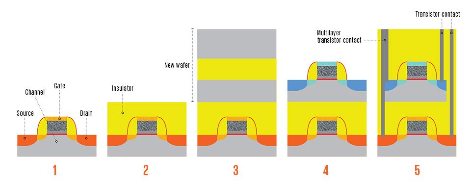
Illustration: Erik VrielinkSecond Story: This monolithic manufacturing scheme, developed by CEA-Leti, builds two tiers of circuitry using silicon from two separate wafers. (Some steps are not shown.)
The first layer of transistors—and the metal wires used to connect them—is built on a silicon wafer.
The circuitry is coated with a layer of oxide to serve as electrical insulation.
A new wafer containing a layer of oxide sandwiched between two layers of silicon, one thick and one thin, is bonded upside down on the first layer.
The bulk of the wafer and oxide are removed, and a second layer of circuitry is built on top of the remaining silicon.
Holes are etched down through the stack and filled with metal. The resulting interconnect can wire two layers together [left] or access each layer individually [right].
But the process is less straightforward than it sounds. Temperatures upwards of 1000 °C are typically used to force dopant atoms into silicon and create the semiconductor portions of the transistor. Applying such heat to create a second layer of transistors could destroy crucial components in the first, including salicide, a metal-silicon alloy used to help carry signals in and out of devices.
Now, research into lower-temperature processes is picking up. Leti has developed one scheme that bonds a second silicon wafer on top of the first tier of circuitry. All but a thin silicon layer on this second wafer is stripped away. A second layer of transistors is built using a process called solid-phase epitaxy, in which a mixture of dopant atoms and amorphous silicon is laid down. The mix is then heated to just 600 °C, giving the silicon enough energy to crystallize. As a last step, connections are made by etching holes down to the first layer and filling them with copper.
This approach has been used to create basic circuits, such as inverters, that span two chip layers. And last year, Leti reported that devices fabricated with this process perform as well as those made at higher temperatures. The work is now getting the attention of chipmakers. In December 2013, during the IEEE International Electron Devices Meeting in Washington, D.C., Leti announced that it had entered into an agreement with mobile chip powerhouse Qualcomm to evaluate the technology for mass production. In the process of this research, Vinet says, Leti worked closely with manufacturing partner STMicroelectronics. “There is no major roadblock to the transfer of this technology to foundries,” she says. “I feel very confident when I say that.”
Leti isn’t the only group exploring monolithic fabrication. At the same meeting, for example, a team led by Jia-Min Shieh of the National Nano Device Laboratories, in Hsinchu, Taiwan, presented two-tier circuits made by growing silicon atop a layer of transistors instead of adding a second silicon wafer. The Taiwan team’s low-temperature process isn’t sufficient to create perfect single-crystal silicon, so the process might be suitable only for creating memory, which tends to be more tolerant of crystal defects, Shieh says.
When it comes to memory, monolithic 3-D fabrication already seems to be making inroads in industry. In August, Samsung announced it had begun production on NAND flash with memory cells arranged along dense vertical lines, and other companies have similar plans. But details are scant on the particulars of the manufacturing process.
“Memory looks like it’s already commercialized. Logic has a long way to go,” says Sung Kyu Lim of Georgia Tech. Lim, who is working on monolithic 3-D circuit design, says there are open questions that can be resolved only when research progresses from simple components to full-size chips. Manufacturing imperfections and variations could lower yield and make monolithic 3-D chips more expensive. He adds that transistors made at lower temperatures may not perform as well as their high-temperature brethren, a shortcoming that would necessitate larger and thus less dense transistors in the upper stages of designs. Still, he says, as chipmakers bump up against fundamental physical limits, they may find themselves short on options. In the future, he says, “the only way to go to add more devices will be vertical.”

Aucun commentaire:
Enregistrer un commentaire